Table of Contents >> Show >> Hide
- FPGA 101: What It Is (and Why It Feels Like Cheating)
- So What Exactly Is an “FPGA Computer”?
- Inside the FPGA: The LEGO Bricks That Become Hardware
- The Toolchain: Where Your Hardware Becomes Real
- A-to-Z FPGA Computer Cheat Sheet
- A Accelerator
- B Bitstream
- C Constraints
- D DSP Slices
- E Embedded (SoC) FPGA
- F Fmax
- G GPIO
- H HDL
- I IP Cores
- J JTAG
- K Kernel (Hardware Kernel)
- L LUT
- M Microarchitecture
- N Networking
- O On-Chip Memory
- P Place & Route
- Q Quartus Prime
- R Reconfigurable Computing
- S Soft Processor
- T Timing Closure
- U UART
- V Vivado / Vitis
- W Workload Fit
- X eXternal DDR
- Y Yield (Debug Yield)
- Z Zynq (and friends)
- Where FPGA Computers Show Up in Real Life
- How to Build Your First FPGA Computer (Without Crying)
- FPGA vs CPU vs GPU vs ASIC: A Practical “Which One?”
- Common Pitfalls (a.k.a. How FPGA Tools Humble Everyone)
- Conclusion: FPGA Computers Are Worth It (Yes, Even With the Learning Curve)
- Field Notes: of Real-World FPGA Computer Experience
If you’ve ever wished your computer could shapeshiftlike a sci-fi robot, but with fewer moral dilemmaswelcome to the world of
FPGA computers. An FPGA (Field-Programmable Gate Array) lets you rewire “hardware” after it’s manufactured. That means you can build
custom accelerators, soft-core CPUs, and weirdly delightful machines that sit somewhere between “computer” and “choose-your-own-adventure.”
This A-to-Z guide breaks down what an FPGA computer is, how it works, what tools you’ll use, and why it’s worth your timeeven if you’ve only
ever “programmed hardware” by turning your monitor off and on again.
FPGA 101: What It Is (and Why It Feels Like Cheating)
Traditional CPUs run instructions. GPUs run lots of instructions in parallel. An FPGA is different: you create the digital circuit itself.
Instead of telling hardware what to do step-by-step, you describe what the hardware is. The result is a design that can be deeply parallel,
low-latency, and deterministic (a fancy way of saying “it behaves the same way every time, like your uncle at Thanksgiving”).
Modern FPGA families also include hard blocksDSP slices for math, on-chip RAM, high-speed transceivers, and sometimes full CPU subsystemsso you
can build systems that look a lot like a conventional computer… except you get to redesign parts of the motherboard with code.
So What Exactly Is an “FPGA Computer”?
The phrase FPGA computer can mean a few things, depending on how ambitious (or sleep-deprived) you are:
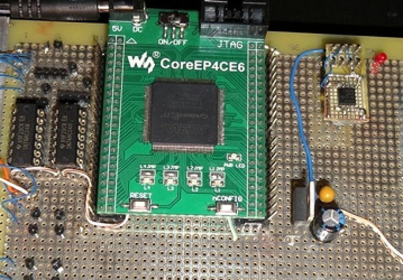
- An FPGA development board acting like a computer: you implement a soft-core CPU (or use a SoC FPGA with hard CPUs), add memory, I/O, and run firmware or even a small OS.
- An accelerator in a larger system: the FPGA lives on a PCIe card or module and speeds up one workload (compression, video, networking, ML inference, search, signal processing, etc.).
- A cloud FPGA instance: you rent FPGA hardware in the cloud and deploy your design remotelyno soldering required, and your lab partner is basically a data center.
The “Computer” Ingredients You’ll Usually Need
- Compute: soft processor (e.g., MicroBlaze/Nios II/RISC-V) or SoC FPGA with embedded CPU cores
- Memory: on-chip BRAM for small/fast buffers; external DDR for real work
- Interconnect: AXI/Avalon buses, crossbars, DMA engines
- I/O: UART, SPI, I²C, Ethernet, USB, HDMI/VGA, PCIe, GPIO
- Boot + storage: flash/QSPI, microSD, bitstream loader
Inside the FPGA: The LEGO Bricks That Become Hardware
Under the hood, an FPGA fabric is made of configurable logic blocks and routing. Your design is turned into a configuration (“bitstream”) that
programs lookup tables (LUTs), flip-flops, routing switches, and other blocks to behave like your circuit.
Key Building Blocks (in plain English)
- LUTs: tiny truth tables that implement combinational logic (AND/OR/mux logic and beyond)
- Flip-flops: storage elements that make sequential logic possible (state machines, pipelines)
- BRAM/URAM: on-chip memory blocks for FIFOs, caches, line buffers, lookup tables
- DSP blocks: fast multiply-accumulate units for filters, codecs, ML layers, control loops
- PLLs/MMCMs: clock managers for generating and conditioning clocks
- High-speed transceivers: SERDES for PCIe, 10/25/100G Ethernet, and other “very fast wires”
The magic is that you can connect these blocks to create a custom datapath. The less magical part is that you also get to debug timing, clocks,
and the occasional “why is my state machine possessed?” moment.
The Toolchain: Where Your Hardware Becomes Real
FPGA development isn’t just “write code and run.” It’s a flow: design entry → simulation → synthesis → place & route → timing closure →
bitstream generation → program device → debug. Different vendors have different ecosystems, but the ideas rhyme.
Major Tool Suites You’ll See in the Wild
- AMD Vivado: design entry, synthesis, place & route, and verification/simulation tooling for AMD adaptive SoCs and FPGAs.
- AMD Vitis: a higher-level development environment that works alongside Vivado, supporting designs that include FPGA fabric, CPU subsystems, and (in some platforms) AI engines.
- Intel Quartus Prime: a full environment for designing FPGAs/SoC FPGAs/CPLDs, including system integration tooling (Platform Designer) and a place-and-route “fitter.”
- Lattice Radiant / Propel: FPGA design tools aimed at efficiency and accessibility, including flows for FPGA-based processor systems.
- Microchip Libero SoC: an integrated suite covering RTL design through programming, with IP libraries and reference designs for Microchip FPGA families.
Translation: you’ll spend time in vendor tools, but you’ll also learn portable fundamentalsHDLs (Verilog/VHDL/SystemVerilog), simulation discipline,
clocking, constraints, bus protocols, and debugging strategy.
A-to-Z FPGA Computer Cheat Sheet
Because sometimes you just need the glossary before your brain agrees to cooperate.
A Accelerator
A custom hardware block that speeds up a specific job (encryption, video, ML inference, packet filtering) by exploiting parallelism and pipelining.
B Bitstream
The configuration file that programs the FPGA fabric. Load it at boot and your “blank chip” becomes your circuit.
C Constraints
Rules that tell tools about clocks, pins, timing requirements, and I/O standards. Forget these and your design may “work” only on Tuesdays.
D DSP Slices
Dedicated arithmetic blocks for fast math. If your FPGA computer touches audio, video, SDR, or ML, you’ll become best friends with DSP blocks.
E Embedded (SoC) FPGA
Devices that combine CPU cores and FPGA fabricgreat for “computer-like” systems where software and custom logic cooperate tightly.
F Fmax
The maximum clock frequency your design can reliably run after place & route. It’s the scoreboardand sometimes the villain.
G GPIO
Basic digital I/O pins. Ideal for LEDs, buttons, and that first “I made hardware do a thing” victory lap.
H HDL
Hardware Description Language. Verilog and VHDL describe hardware behavior and structure. It looks like programming, but it behaves like physics.
I IP Cores
Prebuilt blocks (UART, DDR controllers, Ethernet MACs, PCIe endpoints). You’ll use these to avoid reinventing the wheel… badly.
J JTAG
A common programming/debug interface. Many FPGA boards use USB-JTAG so you can load bitstreams and debug quickly.
K Kernel (Hardware Kernel)
In accelerator workflows, a “kernel” can mean a hardware block (e.g., in higher-level tool flows) that implements a compute function.
L LUT
Lookup table: a configurable logic element. Build enough LUTs together and you can make anything from adders to full CPUs.
M Microarchitecture
Pipelines, state machines, memory hierarchies, and throughput/latency tradeoffs. This is where FPGA performance is actually won.
N Networking
FPGAs shine in low-latency packet processing, encryption, and inline computeespecially when placed directly in the data path.
O On-Chip Memory
BRAM/URAM is fast and close to logic. Great for buffers and caches, but finiteso budget it like it’s vacation days.
P Place & Route
The tool stage that assigns logic to physical resources and routes connections. This is where timing closure dreams go to negotiate.
Q Quartus Prime
Intel’s FPGA design suite used for synthesis, integration, and implementation across many Altera/Intel FPGA families.
R Reconfigurable Computing
The core idea: hardware that can be re-targeted for different tasks, optimizing performance, latency, and power per workload.
S Soft Processor
A CPU implemented inside the FPGA fabric. It won’t beat a desktop CPU at general computing, but it’s fantastic for embedded control and custom I/O.
T Timing Closure
The process of meeting clock constraints. It often involves pipelining, restructuring logic, and choosing battles wisely.
U UART
Serial communication: the “hello world” of embedded interfaces. Perfect for early debugging and printing smug success messages.
V Vivado / Vitis
AMD’s core FPGA design and unified development toolscommonly used for both pure FPGA designs and heterogeneous systems.
W Workload Fit
FPGAs excel when you can exploit parallelism, streaming dataflows, and deterministic latency. Not every problem wants an FPGA. Some problems want a nap.
X eXternal DDR
External memory turns “cute demo” into “useful computer.” It also turns “simple project” into “why is my memory controller angry?”
Y Yield (Debug Yield)
How quickly you can iterate: simulation speed, build times, debug tooling, and your ability to avoid breaking three things while fixing one.
Z Zynq (and friends)
A popular example of a SoC FPGA class: CPU cores plus programmable logicletting software run the show while custom hardware does the heavy lifting.
Where FPGA Computers Show Up in Real Life
Cloud FPGAs: Rent Hardware, Ship Bitstreams
Cloud offerings have made FPGA acceleration far more accessible. For example, AWS introduced FPGA-backed instances with development environments that
support programming, simulation, debugging, and compilation workflows, letting teams deploy hardware acceleration without owning a rack of boards.
More recently, AWS has also described a second-generation FPGA instance line focused on improved price/performance.
Datacenter Acceleration: Inline Compute and Low Latency
At datacenter scale, FPGA fabrics have been used as network-adjacent acceleratorspositioned to touch traffic at line rate and reduce CPU load for
specific tasks. One widely discussed approach places the FPGA between the network and the host, enabling it to act as an inline processor for
distributed workloads.
Embedded + Edge: Determinism Beats Raw GHz
In robotics, industrial control, SDR, and video pipelines, consistent response time matters. FPGA computers can implement custom I/O timing, fast
control loops, and streaming pipelines where latency variance is the enemy.
How to Build Your First FPGA Computer (Without Crying)
Step 1: Pick a Board That Matches Your Goal
If you’re learning, pick a board with good documentation, lots of community examples, and easy I/O (LEDs, buttons, UART, maybe Ethernet).
Popular “trainer” boards often include onboard flash, USB-JTAG, and connectors that make experimentation painless.
Step 2: Start With the Smallest Win: LED Blinking + Simulation
Your first milestone should be an LED blinker and a simulation waveform that matches it. Simulation isn’t optionalit’s how you debug logic before
you’re stuck poking at hardware with hope and vibes.
Step 3: Add a Clock the Right Way
Learn clock constraints early. Define your clock, check timing reports, and understand why “it compiled” is not the same as “it meets timing.”
Step 4: Bring in a Soft CPU (or Use a SoC FPGA)
To make your FPGA feel like a computer, you’ll want a processor:
- Soft CPU route: instantiate a processor core in logic + add memory + peripherals (UART, timer, SPI, GPIO).
- SoC route: use an FPGA with embedded CPU cores for Linux/bare-metal control, and offload custom tasks to programmable logic.
Step 5: Add “Computer Stuff”: Storage and I/O
Add SPI flash or microSD for boot assets. Add UART for logs. Add Ethernet if you want to feel powerful. Add a DMA engine if you want to feel
too powerful.
Step 6: Graduate to a Real Workload
Good first “real” projects for an FPGA computer:
- UART console + command parser + GPIO control
- Simple VGA/HDMI test patterns
- Audio effects (FIR filter, delay)
- Packet counter / basic firewall rules (streaming match)
- Compression block (RLE/LZ-style toy) to learn streaming design
FPGA vs CPU vs GPU vs ASIC: A Practical “Which One?”
Choosing an FPGA is like choosing a vehicle:
- CPU: best for general purpose tasks and fast iteration.
- GPU: best for massively parallel numeric workloads with high arithmetic intensity.
- FPGA: best when you want custom pipelines, low latency, deterministic timing, or specialized I/Oand you can invest in design effort.
- ASIC: best when the design is stable, volume is high, and you need the ultimate efficiency.
In other words: if your workload is a stable, high-volume product, an ASIC might win. If your workload changes, needs low latency, or needs
“hardware that adapts,” FPGA computers become very compelling.
Common Pitfalls (a.k.a. How FPGA Tools Humble Everyone)
- Ignoring constraints: the board “kind of works” until temperature, routing, or clock uncertainty makes it not work.
- Clock domain crossings (CDC): unsynchronized signals between clocks can create intermittent bugs that feel supernatural.
- Timing closure late in the project: pipelining is easier when you plan for it, not when you’re negotiating with a deadline.
- Skipping simulation: debugging only in hardware is slower, noisier, and can lead to creative new swear words.
- Underestimating build time: place & route can take minutes to hours depending on design size and settings.
Conclusion: FPGA Computers Are Worth It (Yes, Even With the Learning Curve)
An FPGA computer is the closest mainstream tech gets to “programmable physics.” You can build custom processors, hardware accelerators, and
deterministic I/O systems that regular CPUs struggle to match in latency and parallelism. The tradeoff is that you must think like a hardware
designer: clocks matter, timing matters, and “works on my machine” becomes “works in my constraints.”
Start small, simulate early, respect timing, and build up from a blinking LED to a soft-CPU system to a real accelerator. Before long, you’ll be
the person who hears “we need lower latency” and replies, “Have you considered… building the circuit?”
Field Notes: of Real-World FPGA Computer Experience
The first time I tried to build an “FPGA computer,” I had a romantic vision: soft CPU, UART console, maybe a tiny graphics output, and a triumphant
moment where my FPGA politely booted like a miniature sci-fi mainframe. Reality showed up wearing a timing report and carrying a chair.
Lesson one: constraints are not paperwork. I once forgot to constrain a clock properly. The design “worked” in the labuntil I
unplugged and replugged the board, or until the room warmed up, or until I looked at it with any confidence whatsoever. Once the clock definition
and pin constraints were correct, half the “mystery bugs” evaporated like morning fog.
Lesson two: simulation is the cheapest truth you’ll ever buy. Early on, I skipped simulation because my logic was “simple.”
That decision cost me an evening of probing signals in hardware, which is like trying to understand a novel by reading three words per page.
When I finally simulated the design, the bug was obvious: a state machine transition depended on a signal that was never asserted in that path.
Ten minutes in simulation could’ve saved two hours of hardware debugging.
Lesson three: clock domain crossings will prank you. I had a UART receiving data in one clock domain and logic consuming it in
another. The system was stable right up until it wasn’tthen it produced corrupted bytes with the confidence of a politician. Adding proper CDC
synchronization (and using FIFOs where appropriate) turned randomness into reliability. It felt less like “fixing a bug” and more like “restoring
the laws of causality.”
Lesson four: timing closure is a design activity, not a final exam. When an FPGA computer grows, long combinational paths sneak in:
address decoding, bus arbitration, or “just one more feature” glued onto the datapath. The cure is usually boring but powerful: pipeline it, register
it, break the path, and accept that latency might increase by a cycle while throughput skyrockets. After the first time you watch Fmax jump because
you added two registers, you start seeing pipelines the way chefs see knives: not optional, but foundational.
Lesson five: iteration speed matters. A full build can take a while, so I learned to structure projects so small changes don’t force
massive rebuilds. I kept reusable IP blocks clean, used incremental builds when available, and reserved “big” place-and-route runs for when the
architecture stabilized. That discipline turned my workflow from “compile and pray” into “iterate and improve.”
The best moment came when my FPGA computer finally behaved like a system: UART console responded instantly, a small hardware accelerator ran in
parallel with the soft CPU, and the design was stable across reboots. It wasn’t magicit was constraints, simulation, CDC hygiene, and a pipeline or
two. But it felt like magic anyway. And honestly, that’s the whole FPGA vibe.