Table of Contents >> Show >> Hide
- Introduction: The Circuit Board Is Not as Flat as It Looks
- What Is LACED?
- Why Peel Back PCB Layers at All?
- The Anatomy of a Multilayer PCB
- How LACED Combines Chemistry and Laser Work
- LACED vs. Manual Sanding: Hope Is Not a Measurement System
- LACED vs. CNC Milling
- What Makes LACED Important for Makers?
- The Role of Imaging and Documentation
- Safety: The Part Nobody Should Skip
- Specific Example: A Six-Layer Board
- Limitations of LACED
- Why LACED Feels Like a Shift
- Experience Notes: What Working Around PCB Delayering Teaches You
- Conclusion: LACED Makes Hidden Hardware More Understandable
Note: This article explains PCB delayering, LACED, chemical etching, and laser-assisted reverse engineering for educational and editorial purposes. It is not a lab manual. Corrosive chemicals, laser systems, PCB dust, and heated resin fumes can be dangerous and should only be handled with proper training, ventilation, protective equipment, and legal authorization.
Introduction: The Circuit Board Is Not as Flat as It Looks
A printed circuit board looks like a tidy little green rectangle until you remember that modern electronics are basically lasagna for electrons. Under the solder mask are copper traces, fiberglass-reinforced epoxy, prepreg, vias, buried layers, power planes, ground planes, and sometimes secrets left by engineers with a sense of humor. That is where LACED, short for Laser-Assisted Controlled Etching and Delayering, becomes fascinating.
The idea behind LACED is simple enough to say and difficult enough to do well: remove a PCB layer by layer using a combination of chemical etching and laser ablation, while documenting each stage so the internal copper structure can be studied. Instead of attacking a multilayer PCB with sandpaper and optimism, LACED uses a low-power diode laser, controlled passes, chemical copper removal, and careful thickness measurement to expose hidden layers with surprising precision.
For hardware reverse engineers, repair specialists, preservationists, and curious makers, this matters because many circuit boards cannot be understood from the outside. If the board is old, rare, undocumented, or deliberately mysterious, the physical PCB may be the only surviving “source code.” Unfortunately, unlike software, you cannot simply open a board in a text editor. You have to peel it like an onion, except the onion is made of glass fiber, copper, epoxy, and tiny grudges.
What Is LACED?
LACED is an accessible approach to PCB delayering, a destructive reverse-engineering technique used to expose and image the individual layers inside a multilayer printed circuit board. Traditional PCB delayering often involves sanding, polishing, milling, microsectioning, X-ray imaging, or industrial failure-analysis equipment. LACED takes a more maker-friendly path by combining inexpensive hardware with controlled chemistry.
The method gained attention because it suggests that meaningful multilayer PCB analysis does not always require a cleanroom, a focused ion beam system, or a budget that makes your wallet leave the room. A small CNC-style diode laser can remove portions of FR4 substrate, while chemicals can strip solder mask and dissolve exposed copper. The key is not brute force. The key is repeatability.
That distinction is important. A milling bit removes whatever sits beneath it: copper, fiberglass, solder mask, dreams, all of it. A diode laser behaves differently. It can char or ablate organic resin and fiberglass composite material, but copper responds very differently because of its reflectivity and thermal conductivity. LACED leans into that behavior by using the laser mainly for dielectric material and chemical etching for copper.
Why Peel Back PCB Layers at All?
PCB reverse engineering is not automatically shady. Yes, the phrase sounds like something whispered in a basement under a flickering fluorescent light, but there are many legitimate reasons to inspect a board’s inner structure.
Recovering Lost Designs
Many companies inherit old products with missing CAD files, obsolete documentation, or suppliers that vanished sometime around the era when beige computers roamed the earth. In those cases, studying the physical PCB can help recreate a schematic, update a design, or manufacture replacement parts.
Repairing and Preserving Hardware
Vintage computers, arcade boards, medical devices, industrial controllers, and lab instruments often depend on PCBs that are no longer available. Delayering can reveal internal traces, hidden vias, and power distribution paths that are impossible to inspect visually from the surface.
Security Research
Hardware security researchers may need to locate debug interfaces, hidden traces, tamper-detection circuits, or undocumented connections. When surface probing is not enough, layer-by-layer imaging can expose how a device is actually wired, not merely how the marketing brochure says it works.
Failure Analysis
Boards can fail due to cracked vias, delamination, corrosion, manufacturing defects, or thermal stress. Controlled delayering helps reveal whether the issue is on the surface or buried deep inside the stackup.
The Anatomy of a Multilayer PCB
To understand why LACED is clever, it helps to understand what is being removed. A typical rigid PCB is built from copper foil laminated to insulating material, usually FR4: a composite of woven fiberglass cloth and epoxy resin. In a multilayer board, copper layers are stacked with core and prepreg materials, then pressed together under heat and pressure. The final board is drilled, plated, masked, printed, finished, and assembled.
A simple two-layer PCB has copper on the top and bottom. A four-layer board may add internal power and ground planes. A six-layer, eight-layer, or twelve-layer board can contain dense signal routing, impedance-controlled traces, buried planes, and via structures that make the outside view wildly incomplete.
In other words, the top layer tells only part of the story. Sometimes it tells the boring part. The drama is inside.
How LACED Combines Chemistry and Laser Work
LACED works because it divides the job according to material. Solder mask, copper, and FR4 do not behave the same way, so forcing one removal method to handle everything is asking for trouble. The process uses different tools for different layers.
Removing the Solder Mask
The solder mask is the colored protective coating on the outside of the PCB, most commonly green, though modern boards may be black, red, blue, purple, white, or the ever-fashionable “mysterious matte finish that hides everything.” It protects copper from oxidation and helps prevent solder bridges during assembly.
For reverse engineering, the solder mask gets in the way. LACED uses chemical softening or stripping to expose the copper beneath it. This is where safety becomes non-negotiable: chemicals used for solder mask removal can be caustic, and fumes or splashes can cause serious injury. The editorial takeaway is not “try this in the kitchen.” The takeaway is that controlled chemical preparation can produce a more uniform surface than scraping with a knife while muttering motivational phrases.
Dissolving Copper with Chemical Etching
Once copper is exposed, LACED uses chemical etching to remove it selectively. Copper etching is already a familiar idea in PCB manufacturing: unwanted copper is dissolved away, leaving the intended traces behind. LACED flips the normal goal. Instead of preserving a trace pattern, the goal may be to remove a copper layer so the next dielectric layer can be accessed and imaged.
This is one of the reasons LACED is interesting. Mechanical abrasion can easily smear, gouge, or tear features. Chemical copper removal, when controlled properly, can avoid some mechanical damage and reduce the risk of a tool plowing through a fine trace like a tiny bulldozer with no emotional intelligence.
Laser Ablation of FR4
After copper is removed, the remaining FR4 or dielectric material must be thinned or opened to reveal the next copper layer. A low-power diode laser can ablate resin-rich material in controlled passes. The operator can measure thickness changes after each pass and adjust the process gradually.
The strength of this method is precision. Manual sanding depends on pressure, grit, flatness, patience, and whether your hand had too much coffee. A CNC-guided laser offers more consistent motion. That does not make it magically easy. Laser settings, focus, scan spacing, heat buildup, soot, and carbonization all matter. Push too hard and the FR4 chars. Go too slowly and heat spreads. Get careless and delicate copper features may lift, warp, or disappear from the narrative.
LACED vs. Manual Sanding: Hope Is Not a Measurement System
Manual sanding is the classic low-budget PCB delayering method. It can work, especially on simple boards, and it requires very little equipment. The process is straightforward: remove material gradually, clean the surface, inspect the layer, photograph it, repeat. The problem is that “gradually” is doing a heroic amount of work in that sentence.
Human hands are not precision Z-axis systems. Pressure varies. Sandpaper loads unevenly. Corners disappear faster than the center. One extra stroke can turn an internal trace into copper confetti. If the goal is to expose a broad plane, sanding may be good enough. If the goal is micron-scale layer control, sanding becomes less like engineering and more like archaeology performed with a cheese grater.
LACED improves on that by introducing measurable passes, consistent tool motion, and a material-specific strategy. The laser attacks the dielectric. Chemistry handles copper. A micrometer tracks progress. The process still requires judgment, but it replaces some guesswork with data.
LACED vs. CNC Milling
CNC milling can remove PCB material with excellent positional control, but it is mechanically aggressive. A carbide bit does not politely stop because it has reached copper. It cuts whatever is in the way. For PCB reverse engineering, that can be a problem because the very features being studied are fragile.
A milling setup also introduces vibration, tool wear, surface ridges, and alignment challenges. With a sufficiently good machine, careful fixturing, and proper tooling, CNC delayering can be powerful. But consumer-grade machines may struggle with the combination of flatness, depth control, and feature preservation required for fine multilayer analysis.
LACED’s advantage is not that it makes all other methods obsolete. It does not. Its advantage is that it offers a lower-cost, non-contact approach for portions of the process, using the laser where it is useful and chemistry where the laser is not.
What Makes LACED Important for Makers?
The maker community loves tools that move a process from “only a lab can do this” to “a careful person can learn this.” LACED fits that pattern. It does not trivialize PCB reverse engineering, but it lowers the intimidation factor. A low-cost diode laser engraver, careful measurement, scanning, and controlled documentation can produce meaningful results when used responsibly.
That matters because electronics are increasingly sealed, undocumented, and disposable. Devices fail, companies disappear, and boards become black boxes. Open, reproducible delayering methods help people understand technology instead of treating every object as magical plastic with a charging port.
The Role of Imaging and Documentation
Delayering is only half the job. The other half is documentation. Each exposed layer must be cleaned, scanned or photographed, aligned, and interpreted. Without good imaging, the result is just a damaged PCB and a story beginning with “Well, it looked clearer in person.”
A practical workflow includes imaging the original board, both sides, before modification. Then each stage is captured again after solder mask removal, copper etching, dielectric removal, and exposure of each new layer. Alignment holes, vias, board edges, and component footprints can help register images so the layers can be compared in software.
Once aligned, the images reveal nets, planes, routing channels, stitching vias, and design choices. A reverse engineer may trace power rails, identify memory bus routing, locate a hidden UART, or understand why a board was designed with a particular stackup. The PCB becomes readable, though still not exactly bedtime reading unless your dreams contain impedance discontinuities.
Safety: The Part Nobody Should Skip
Any discussion of LACED must include safety. FR4 dust and fumes are not friendly. Heated epoxy resin can release irritating or hazardous compounds. Fiberglass particles are not something you want in your lungs. Corrosive chemicals can damage skin, eyes, lungs, tools, sinks, and your relationship with whoever owns the table you just ruined.
Laser safety is equally serious. Protective eyewear must match the laser wavelength. Reflections can be dangerous. Smoke extraction matters. Fire risk is real. The phrase “just a 5-watt diode laser” can create false confidence; a low-cost laser is still a device designed to concentrate energy into a small spot. It deserves respect.
Chemical handling requires ventilation, compatible containers, labeling, spill planning, and proper disposal. Used copper etchant is not ordinary household waste. It contains dissolved metals and must be treated according to local regulations. The best reverse-engineering project is the one where the board gets destroyed, not the operator.
Specific Example: A Six-Layer Board
Imagine a six-layer PCB from an old solid-state drive or embedded controller. The surface reveals components, pads, and visible traces, but much of the routing disappears into vias. A researcher wants to understand how signals travel between the controller, memory, power regulation, and external connector.
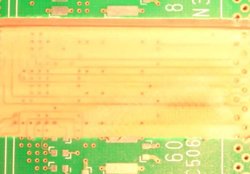
The board is first scanned to preserve the visible top and bottom layers. The solder mask is removed so copper can be documented clearly. The outer copper layer is chemically etched away. The dielectric beneath is then thinned with controlled laser passes, with measurements taken between passes. When the next copper layer becomes visible, the board is cleaned and imaged again. The cycle continues.
By the end, the board is physically sacrificed, but its structure has been converted into a layer-by-layer visual record. That record may allow reconstruction of major nets, hidden planes, routing strategies, and design intent. The board is gone, but its secrets have been persuaded to leave a forwarding address.
Limitations of LACED
LACED is impressive, but it is not magic. It is destructive. It is slow. It requires calibration. It may not work equally well on every solder mask, laminate, copper weight, resin system, board thickness, or layer count. Some PCBs include buried vias, microvias, filled vias, heavy copper, blind structures, unusual laminates, or high-frequency materials that complicate the process.
The technique also requires a disciplined imaging workflow. Without consistent lighting, focus, scaling, and alignment, the exposed layers may be difficult to interpret. A beautiful delayering job can still produce poor data if the images are blurry or distorted.
Finally, chemical and laser processes introduce risk. Accessibility is not the same as casualness. A low-cost setup can be powerful, but it still demands planning, testing, ventilation, PPE, and patience.
Why LACED Feels Like a Shift
The most exciting part of LACED is not merely that it removes layers. People have been delayering boards for years. The exciting part is the mindset: use affordable tools intelligently, understand the material science, document the process, and share the method openly enough for others to improve it.
This is how technical communities progress. Someone tries the difficult thing. They fail repeatedly. They discover that copper behaves differently from FR4, that heat causes carbonization, that measurements matter, and that “good enough” becomes better when repeated carefully. Then they publish the lessons so the next person starts several mistakes ahead.
Experience Notes: What Working Around PCB Delayering Teaches You
The first lesson from any PCB delayering project is humility. A circuit board may look flat, but it is a compressed history of manufacturing decisions. Every layer exists because someone had to route signals, manage return paths, reduce noise, distribute power, pass compliance tests, fit a shape, or hit a price target. When you peel a board back, you are reading those decisions in reverse.
The second lesson is that patience beats force. Beginners often want the process to move faster. More power, more pressure, stronger chemistry, longer exposure: all of these sound tempting until the layer you wanted turns into a scorched abstract painting. PCB delayering rewards tiny steps. Remove a little. Clean. Inspect. Measure. Image. Repeat. It is less like demolition and more like restoring a fossil, except the fossil once ran firmware.
The third lesson is that documentation must start before the exciting part. Take images before removing anything. Capture both sides. Note orientation. Mark reference points. Record measurements. Save settings. The moment you think, “I’ll remember this,” you have created a future mystery. You will not remember. The board will not remind you. The tiny via near the corner will laugh silently.
The fourth lesson is that lighting changes everything. Copper can look bright, dark, invisible, or suspiciously like a coffee stain depending on angle and surface condition. Cross-lighting, flatbed scanning, macro photography, and careful cleaning can reveal details that are otherwise lost. Sometimes the improvement from better imaging is greater than the improvement from more aggressive delayering.
The fifth lesson is that every board has its own personality. Some solder masks come off cleanly. Others cling like they signed a long-term lease. Some copper layers etch evenly. Others expose strange patches, residue, or undercutting. FR4 from one manufacturer may ablate differently from another. Older boards, high-temperature laminates, heavy copper designs, and densely filled ground planes all behave differently. There is no universal “one setting to rule them all.”
The sixth lesson is that safety slows you down in exactly the right way. Wearing proper eye protection, checking ventilation, labeling containers, waiting for fumes to clear, and cleaning residues may feel tedious, but they create the discipline that good delayering already requires. Carelessness shows up twice: first in the lab, then in the data.
The seventh lesson is that LACED is valuable even when it fails. A failed pass teaches how a laminate chars, how copper lifts, how much soot blocks imaging, or how measurement error creeps into the workflow. The best experiment logs include ugly results because ugly results are where the method becomes real. Anyone can present the perfect exposed layer. The useful knowledge is often hiding in the ruined sample beside it.
Finally, PCB delayering changes how you look at electronics. After seeing the internal layers of a board, you stop thinking of a PCB as a flat object. You start seeing it as a three-dimensional electrical city: surface roads, underground tunnels, power reservoirs, ground highways, and vias acting like elevators between floors. LACED gives makers and researchers a way to tour that city without needing industrial equipment. It is slow, destructive, messy, and oddly beautiful. In other words, it is hardware hacking at its most honest.
Conclusion: LACED Makes Hidden Hardware More Understandable
LACED is not a shortcut for careless reverse engineering. It is a controlled approach to a difficult problem: exposing multilayer PCB structures without relying entirely on manual sanding or expensive industrial systems. By combining chemical etching, laser ablation, careful measurement, and documentation, it gives researchers and makers a practical path toward understanding what lies inside complex circuit boards.
The method’s real value is not only technical. It represents a broader movement toward accessible hardware analysis. As devices become harder to repair, document, and preserve, techniques like LACED help shift knowledge back into the hands of people willing to study, measure, and share. A PCB may be laminated shut, but with the right method, its layers can still tell their story.